
HP3478A FRAM mod
Because I had already lost my calibration of the meter by taking out the SRAM backup battery for shipping purposes I was able to try to implement an idea/modification I had in my head for a longer time. I really disliked the idea of buying a new lithium battery for my meter and to install it, especially because I know that there are much better options nowadays. This is when I decided to modify my 3478A meters to use FRAM (ferreromagnetic RAM) instead of the original battery-backed up SRAM solution. FRAM acts like normal SRAM, with the big difference that FRAM does not loose the data when it is powered down. I have never used FRAM before, and this was the perfect occasion to learn and try out something new.
 Please keep the following in mind: Removing the battery, shorting the RAM supply voltage only for a split second or doing anything else shown on this page will result in lost RAM calibration constants. This will turn a still valueable and useful meter into a less valueable and useful one! Also handle the lithium battery contained in the 3478A with care. Never short the battery and be aware of the fire hazard. For disposal of batteries always follow safety guidlines and the industry/government rules/guidlines in your state.
The SRAM used in the 3478A to store the calibration data is 256 words long, and each word consists of 4 bits. First step was to find a FRAM replacement with a supply voltage of 5V and with a parallel data bus. Because most FRAM devices work with a serial bus interface this task was not so easy. After some time I decided to use the FM18W08 FRAM from Cypress Semiconductor which consists of 32k words of 8 bits. Price tag for this device is 12 Euros, and therefore buying a new battery would most likely be cheaper, but saving money is not the idea behind this modification. After buying the new memory the first step will be to learn more about the databus in the 3478A.
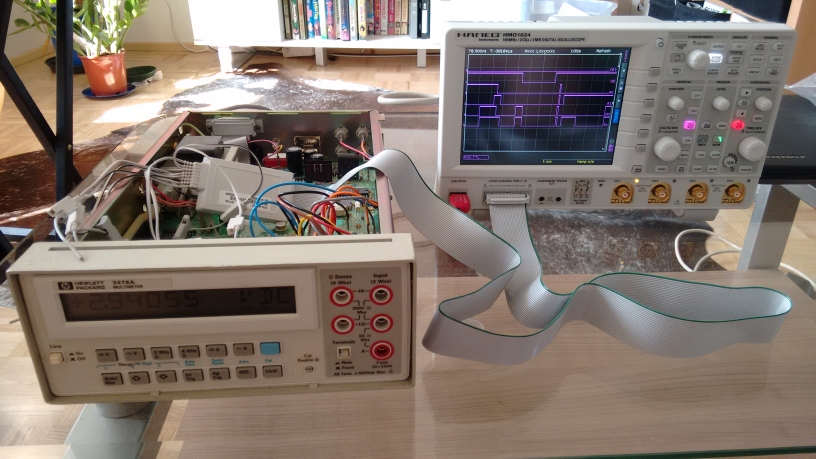
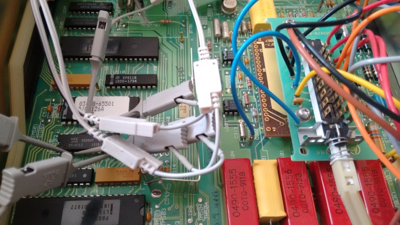
Tool of choice for this bus timing investigation is my Hameg HMO1024 using the digital POD. I decided to monitor the /CE1 and OD signal, plus two additional adress bus and data lines. After turning the 3478A on my first finding was that the meter continiously reads from the SRAM. My expection was always that the microprozessor probably reads the contents from the SRAM during startup into variables and then the bus access to the SRAM stops. But instead it seems that for every measurement cycle the calibration data is directly read from the calibration SRAM.
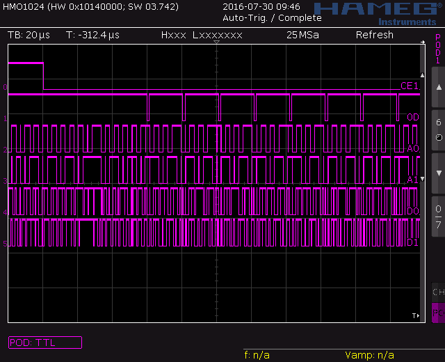

The left picture above shows a series of read accesses from the calibration SRAM. The right picture shows in detail how a single read access is done bus timing wise. First the microprozessor selects the SRAM device by asserting the /CE1 chip select signal, and then all read accesses are done by first updating the adress bus information, and last but not least the /OD (output drive) signal goes low to enable the output drivers from the SRAM device. At the same time the microprozessor reads back the data from the databus. After all data is read and a read cycle is finished the SRAM is deselected again by a low-to-high transition of /CE1.
Interfacing FRAM
My first plan was to directly connect the FRAM to the 3478A bus. I made sure that the logic levels are correct, and I also used a device which control signals looked correct for a direct replacement of the original SRAM. But after reading the FRAM datasheet I spoted a small problem. It seems that FRAM devices in general have a small timing requirement which is different to normal SRAM: The new device requires a falling edge on the /CE chip select signal to latch in the adress information for every next read or write cycle. The datasheet of the FM18W08 talks in detail about this difference and that there are widely used bus timing schemes which are not compatible. The original SRAM used in the 3478A does not have this requirement, and as it turned out the original unmodified bus timing on this 3478A data bus is not compatible, because the microprozessor does not generate a falling edge on /CE1 for every read/write cycle.Because I was still determined to make this modification I decided to use some glue-logic to generate a compatible timing scheme for the FRAM. The used circuitry is shown below. Because the new RAM had so much more adress-space than I needed some adress lines were simply not used, and I was also able to implement a nice feature: A BCD switch sets four adress-lines of the RAM and allows me to select one out of 16 possible calibration banks. I only use the four lowest bits of the data bus, the other data lines of the RAM are simply tied down with pulldown resistors. I installed some series resistors on the lower data bus bit lines to prevent damage to devices on the 3478A data bus in case I would get bus collisions during my first attempts.

Modification
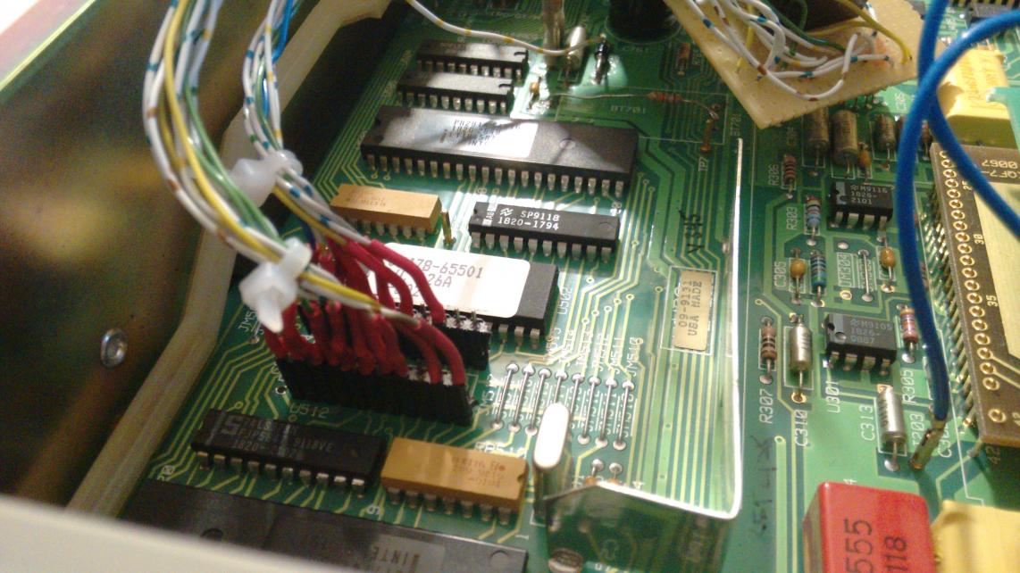
First step for the modification was to deactivate the old RAM device. My first plan was to only disconnect the /OD signal and to leave the old RAM intact and in place in case my idea does not work. This would allow me to easily go back to the original circuitry. Unfortunetly it was much more difficult than I expected to disconnect the /OD signal from the RAM and I decided to remove the old device altogether. I completely desoldered the old SRAM and installed pinheaders instead. When I switched on the 3478A without any RAM in place at all I simply got the message Uncalibrated: it seems that the 3478A does not recognize that the RAM was missing completely.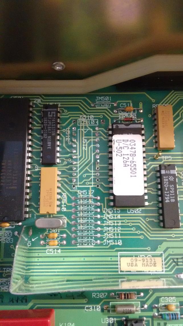
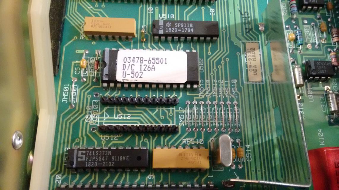
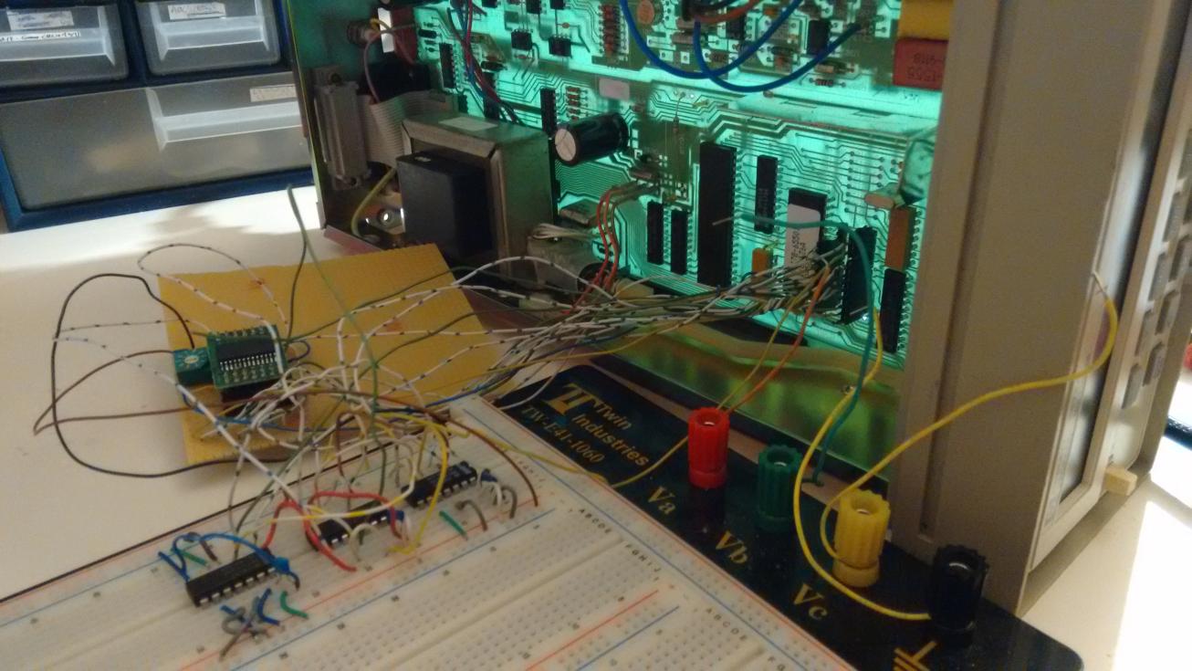
The FM18W08 comes in a 28pin SOIC package: I decided to use a SOIC to pinheader adapter board to allow easy prototyping. This also has the advantage that the RAM is now easy interchangable. If I want to read the contents from my computer I can simply remove it from the 3478A and install it on another circuit for data access. During initial prototyping the glue-logic was tested on a breadboard. Later this circuitry was rebuilt on veroboard including the pinheaders for the FRAM. The connections to the 3478A itself were made using wires which are routed to the newly installed U512 pinheaders. Power to the glue-logic and the FRAM is supplied also via the U512 power supply pin.
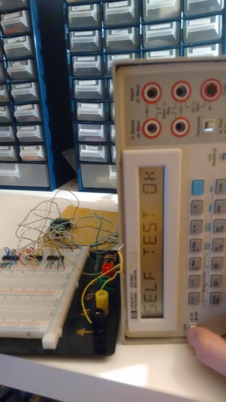
The initial test setup is shown below. After switching on my 3478A the first time after the modifications were done I still got the Uncalibrated message on the display as expected. Now I used my DIY calibrator circuit and the standard calibration procedure to "calibrate" the 3478A. After finishing the calibration procedure I restarted the 3478A and I was very happy that I was welcomed with the "Self Test OK" message again. This was the prove that the microprozessor is able to correctly read and write to the calibration RAM via my glue-logic. It was also interesting to use the "calibration bank selection BCD switch". When I selected the next bank and started the 3478A I was again received by a Uncalibrated message. After moving back to bank 0 my meter was calibrated again.
FRAM bus signals
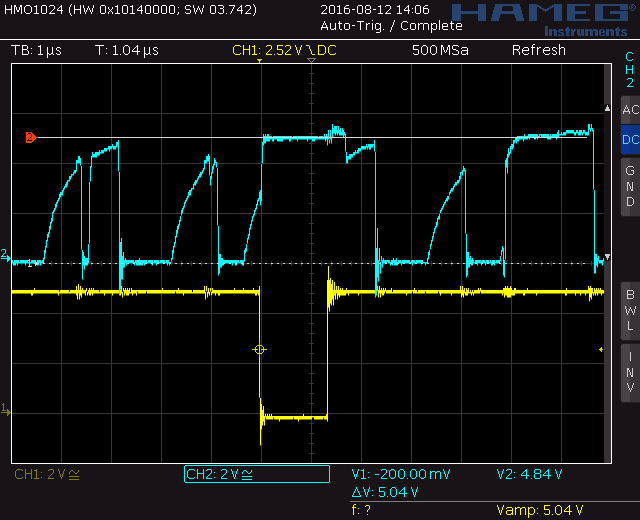
The following pictures show the timing of the bus signals again, this time on the control pins of the FRAM during read accesses. This allows to compare the signals to the original ones at the top of this page. The glue-logic makes sure that for every write/read access to the FRAM we get the needed falling edge on /CE chip enable signal before. I also added a picture showing data line D0 during a read access on the 3478A data bus to make sure that there are no problems with the logic levels: CH2 shows D0 (light blue), CH1 shows /OE signal on the FRAM (yellow) and is also used to trigger on the read access. This third scope picture reveals that everything is OK with the digital signal levels.

3478A reset circuitry
The 3478A service manual shows a detail which is important when removing the SRAM backup battery completely: The reset circuitry uses the always present battery voltage to generate a proper reset signal during powerup of the meter. This is done by using a comparator which compares the still unregulated +5V supply voltage rail (voltage before the 5V linear regulator for the digital section) with the always present battery voltage. During startup when the unregulated supply voltage will start at 0V and will slowly ramp up the battery voltage is always bigger, and the comparator will pull its output low. This low level keeps the microprozessor in reset state and also makes sure that the calibration RAM can not be selected via CE2 signal. This is important because this prevents accidently writing and destroying the RAM calibration data during startup or power loss. As soon as the unregulated +5V voltage is high enough the divided down voltage exceeds the battery voltage, the comparator flips into the other output state, and the reset line of the microprozessor and CE2 of the calibration RAM are pulled high by a internal pullup resistor in the microprozessor. This ends the reset-state and the microprozessor starts to work.The 3478A also has a watchdog timer which is reseted periodically by the microprozessor during normal operation (keyboard scan signal resets the watchdog counter) and the watchdog timer reset requests are also handled by a second comparator not shown in the picture below. Both comparators are in the same device and have open-collector outputs. This allows to tie both reset request outputs together in a wired-or configuration. The whole reset topology of the 3478A is shown in the left picture below. The right picture shows an additional circuit I added to generate a proper reset signal even though the battery is not installed anymore.
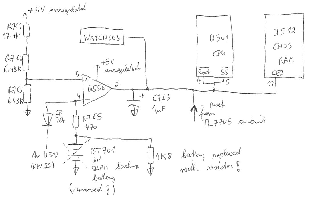

I removed the SRAM backup battery completely and replaced it with a 1.8k resistor to make sure that the input signal to the comparator U550 is always properly defined. The problem is now that the reset signal generation idea in the 3478A does not properly work anymore: the negative comparison input to the U550 comparator is always 0V, and this means as soon as the unregulated +5V supply rail voltage ramps up the comparator releases its output and the microprozessor can start to work, even though the supply voltage is still not ramped up far enough. This can lead to startup problems or calibration RAM data corruption. To fix this issue I added another small circuit with a TL7705 brownout-detector & reset generator from Texas Instruments. This device only deasserts the reset output signal when the voltage on the Sense input pin is high enough. This Sense pin is connected to the regulated +5V supply voltage which is also used by the microprozessor. A timing capacitor Cx allows to set a minimum duration for the reset pulse. Because the /RESET pin of the TL7705 is also an open-collector output it can simply be wired-or with the other 3478A reset comparator outputs.
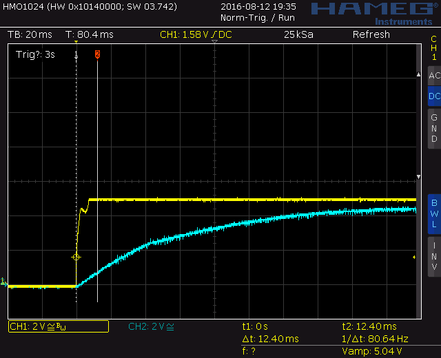
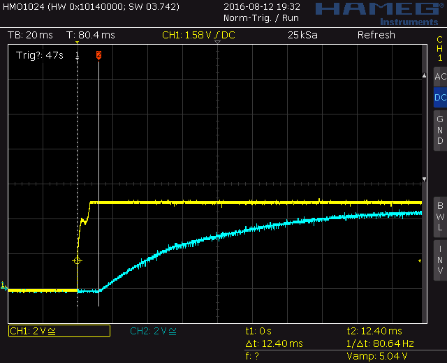
The difference in 3478A reset behaviour between TL7705 circuit missing and circuit added can be seen below. Both pictures show the +5V regulated digital supply voltage on CH1 (yellow), and the voltage on the reset signal at pin 2 of U550 on CH2 (blue). In the left picture the TL7705 is missing and the reset signal start to ramp up even though the +5V supply voltage is still ramping up. This could lead to problems. In the right picture the proposed TL7705 reset control circuit was added, and this circuit makes sure that the reset signal is only deasserted after the +5V digital supply voltage is sufficient and the reset pulse duration time set by capacitor Cx has elapsed.
Assembly
The necessary circuitry was constructed on Veroboard. Then everything was connected again to the 3478A PCB via the U512 socket. The only wire connection between the PCB and the 3478A which can not be routed via the U512 socket is the digital +5V supply rail for the reset generation circuit. The +5V supply trace on pin 22 of the U512 socket can not be used for supply of the reset circuitry because this voltage is already decreased by a diode drop. If this supply pin would be used then the reset generation circuit would keep the meter in endless reset state, because the supply voltage does not reach the necessary threshold. To solve this a direct wire connection between the PCB and the 3478A board taps of the full +5V digital supply rail voltage for the reset generation circuitry. The FRAM and glue logic is supplied via pin 22 on the U512 socket like the SRAM device before. The final board and 3478A assembly is shown below.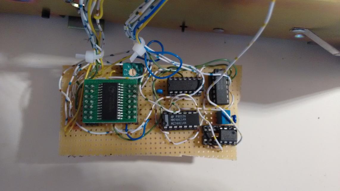

The last question was how to install the new FRAM PCB inside the meter. Unfortunetly with the size of the PCB (using veroboard and throughhole components) and the space restrictions in the meter I was not able to find a professional looking solution. The FRAM PCB was put into a box to prevent shorts and then "installed" in the empty space inside the meter. Because I know I will never sell my meter this solution is good enough for me right now. If for whatever reason I decide one day to return to the original SRAM circuitry again this modification can also be reverted: I would just need to buy and solder in a new SRAM device. Unfortunetly the get harder to find and will cost you also 8 euros or more.
Back to the 3478A page