
DIY Phase Locked Loop
Why
If you ever wanted to built a phase locked loop from scratch for experimentation or to simply learn more about it, using only jellybean parts and not winding a single inductor then this page shows you how you can do it. Granted the performance of this PLL is poor in comparison what you can get by simply spending some bucks on a finished integrated circuit but still it will be functional and a good showcase of how all the blocks work together. To simplify the circuit the shown PLL will be an integer design, that means we only use feedback divider ratios which are an integer number.Voltage controlled oscillator (VCO)
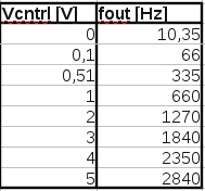
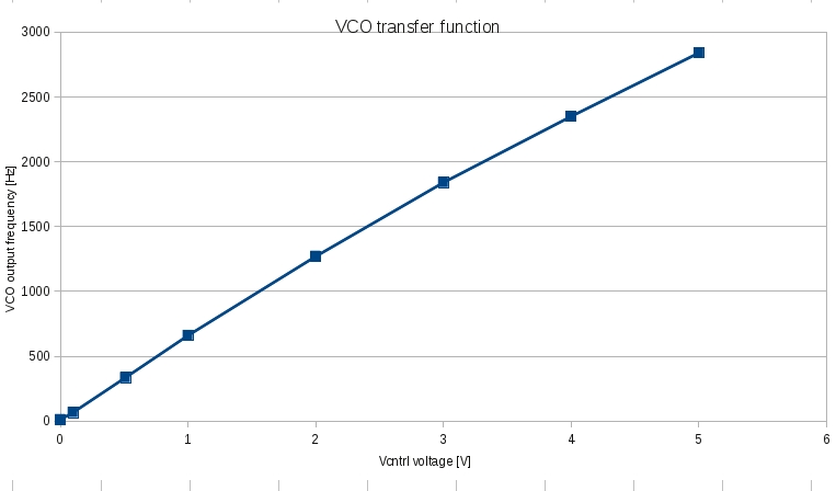
Heart of the phase locked loop is the voltage controlled oscillator. It allows the PLL to generate its output signal. The output frequency is controlled by the VCO control input voltage and can be varied within a certain range (tuning range). For this example I decided to use an opamp based relaxation oscillator for the VCO, because it is very straight-forward, does not require an inductor and if the circuit is put together properly oscillation will start for sure. Drawback of course is the relatively unstable output frequency. The VCO is based on a LM324 opamp using a +5V single supply and produces a triangular and a rectangular output signal. The rectangular signal allows easy frequency division in the feedback path. The VCO circuitry is shown below with a measurement result for the VCO transfer function.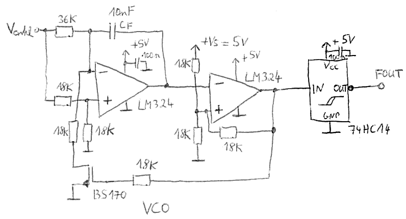
First the VCO rectangular opamp output signal was directly connected to the divider input, but the divider was not working. I only got random spikes at the divider output, but not the expected rectangular output signal. After debugging I found out that the problem is that the opamp rectangular output signal has a limited rise time, and because of this it triggers the divider more than one time during the rising edge of the signal. If the divider triggers two times during one rising clock signal edge the divider flip-flop output flips back to the state that it had before, and only a short spike is visible at the output. To solve this problem the input signal to the divider needs much faster rise and fall times, and by using a 74HC14 Schmitt-Trigger on the VCO output a proper signal is generated.
Phase frequency detector (PFD / CP)
Brain of the phase locked loop is the phase detector which continiously compares the phase of the reference input signal and the feedback signal from the VCO/divider. Depending on the phase difference on its intput it adjusts the input control voltage (tune voltage) of the voltage controlled oscillator to minimize the phase difference over time. There are two conditions that have to be fullfilled to be able to reach zero phase difference between reference lock signal and the output signal: First and most important the frequency of both signals must be identical, and if this is not the case then constant zero phase difference is not possible.Secondly if the frequency matches the phase detector will control the VCO in a way that the zero phase difference condition is achieved and maintained over time. This locked condition can be maintained as long as no big and fast change in the loop setup is done (for example feedback divider change). This PLL will use a so called phase frequency detector (also sometimes refered to as charge pump), with the big advantage that this detector can correct both a wrong output frequency or a non-zero phase shift. The alternative name "charge pump" seems to be a little bit weird at the beginning, but I think it is derived from the fact that the output stage of this detector transfers current pulses (a defined quantity of charge) into an output capacitor. This capacitor is part of the loop filter and therefore shown in the loop filter section.

The 1N4148 diodes in combination with the transistors form two simple current sources. The flip flop outputs control which of the two current sources are currently switched on. The 74HC00 gates in series generate a certain reset signal delay which sets a certain minimum pulse length for the current pulses. This affects the behaviour of the PLL during the static condition.
Loop filter (LF)
The loop filter makes sure that the PLL as a control system is stable at all times. By changing the loop filter component values we can set a certain PLL bandwidth and alter the dynamical behaviour of the loop. It has to be noted that the control voltage input of the VCO is rather low ohmic and that we can not directly connect this input to the loop filter output. In this case we would load the loop filter too much, and the loop filter transfer function would be altered. To prevent this the last remaining unused LM324 opamp section is used as a buffer amplifier.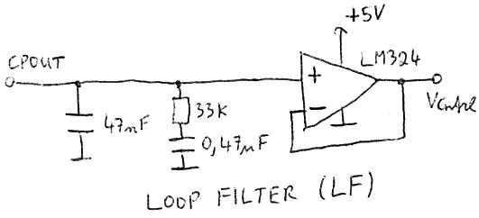
The 47nF capacitor in combination with the output current sources of the PFD form an integrator. Control System wise the VCO is also modeled as a integrator. The resistor and capacitor in series form an additional zero in the frequency response which is necessary to generate additional phase reserve to make the loop stable. Otherwise having only two integrators in the loop would make the loop unstable, because each integrator creates 90 deg phase shift. The loop filter component values which are shown here were not derived by simulation or calculation, but instead by a more experimental approach.
Reference oscillator
Based on a relaxation oscillator with one remaining opamp in the LM324 device. Because this is a demonstration PLL for learning purposes the phase noise of the reference oscillator does not really matter and I just wanted to go for the easiest possible implementation. In practical PLL setups the reference oscillator will be a much more stable clock source or crystal oscillator. Reason is that the phase noise on the PLL output inside the PLL bandwidth will be determined by the phase noise of the reference source. As already described in the VCO section a 74HC14 Schmitt-Trigger was needed at the output to make sure that the rise and fall times of the rectangular signal are fast enough for the used logic gates.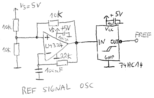
Feedback divider
To demonstrate the function of this basic phase locked loop I want to generate an output frequency which is exactly twice of the reference input signal frequency. The phase detector wants to make sure that its two input signal frequencies are identical. If we divide the VCO output frequency by exactly a factor of 2, and we feed this signal back into the phase detector we force that the loop generates an output frequency which is twice of the reference input frequency. The divider itself consists of a D-FF where the /Q output is feed back into the D input. The divider input signal triggers the D-FF via the clock input. In this configuration the flip flop divides the frequency exactly by a factor of 2.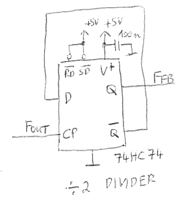
Overall loop
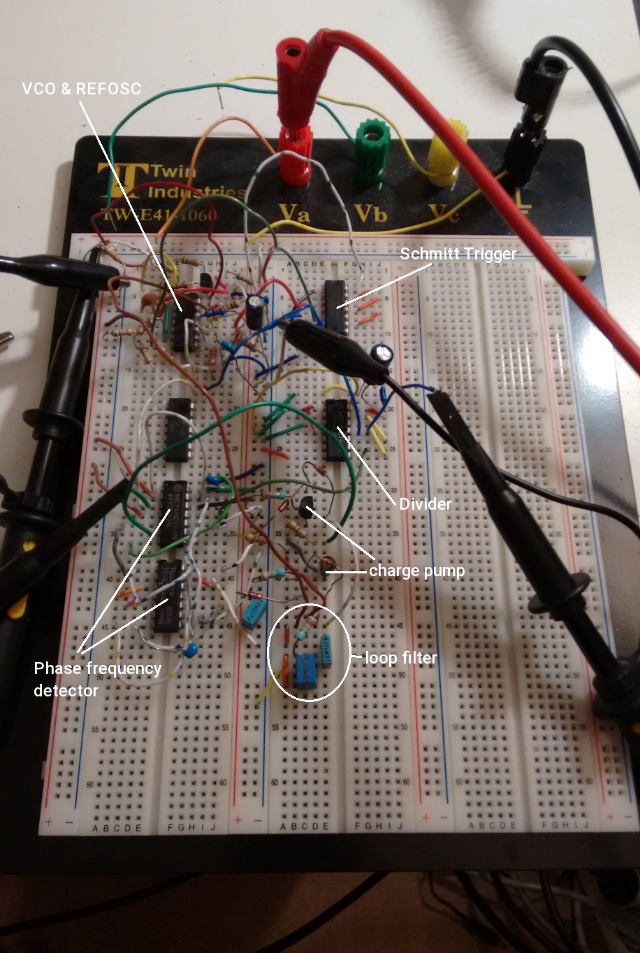
The following picture demonstrates how the final loop is put together from the different building blocks. I build the whole phase-locked loop on a breadboard. A small additional electrolytic capacitor not shown in the schematic above was added to the supply rail on the breadboard to make sure that we also have a small local energy storage for faster transients. The picture of my setup is shown below.
Operation
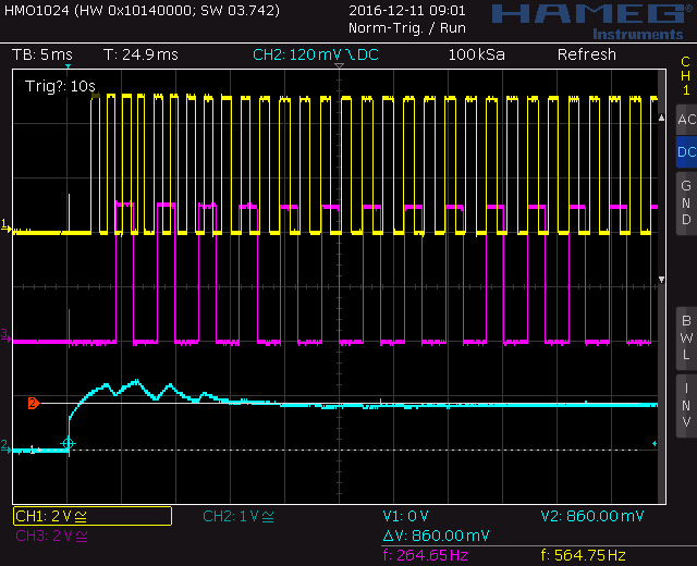
Divide by 2, Output frequency = FRef * 2The loop configuration is using a feedback divider divide by 2 as shown above. The output frequency of the PLL is two times the input frequency. Measured overall circuit current consumption is 1.52mA at a supply voltage of 5V. The control voltage for the VCO settles at approx. 0.85V. The two plots below show the behaviour of the phase-locked loop during initial startup and for the static settled operation. CH1 shows the PLL output signal, CH2 the VCO control input voltage after the loop filter, and CH3 shows the reference input signal to the PLL. The scope plots also show the measured input and output frequency with 274.17 Hz and respective 548.44 Hz. If we calculate the ratio between them we get approx. 2,00036. Please also note that the rising-edges of the input and output signal during the static operation always happen at the same time, and that the signals are therefore "phase-locked" to each other.

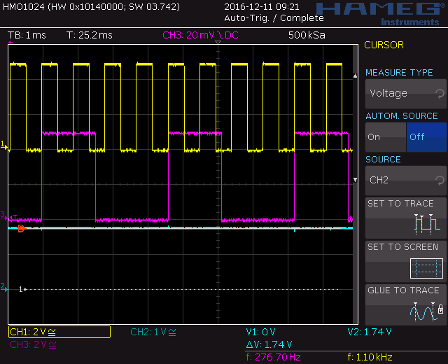
Divide by 4, Output frequency = FRef * 4
By using also the second D-flip flop in the 74HC74 another divide by 2 divider is added to the feedback divider chain. This means the VCO output signal is now divided by 4 before it reaches the phase frequency detector input again. This means we now expect a PLL output frequency of 4 times the input reference frequency. In this configuration the overall circuit draws 1.54mA @ 5V. The VCO control voltage settles to 1.76V. The measured input reference frequency is 276.7 Hz, the measured output frequency reads 1100 Hz. This gives us a factor of approx. 4 (3,975). Reason for the discrepancy is the limited resolution of the scope frequency measurement.

If we compare the two measurement results for the VCO control voltage and output frequency for the closed loop operation case with the VCO open loop transfer function from above this data must match together. The plot below shows that this is the case and that everything worked out exactly as expected.
